.jpg.JPG)
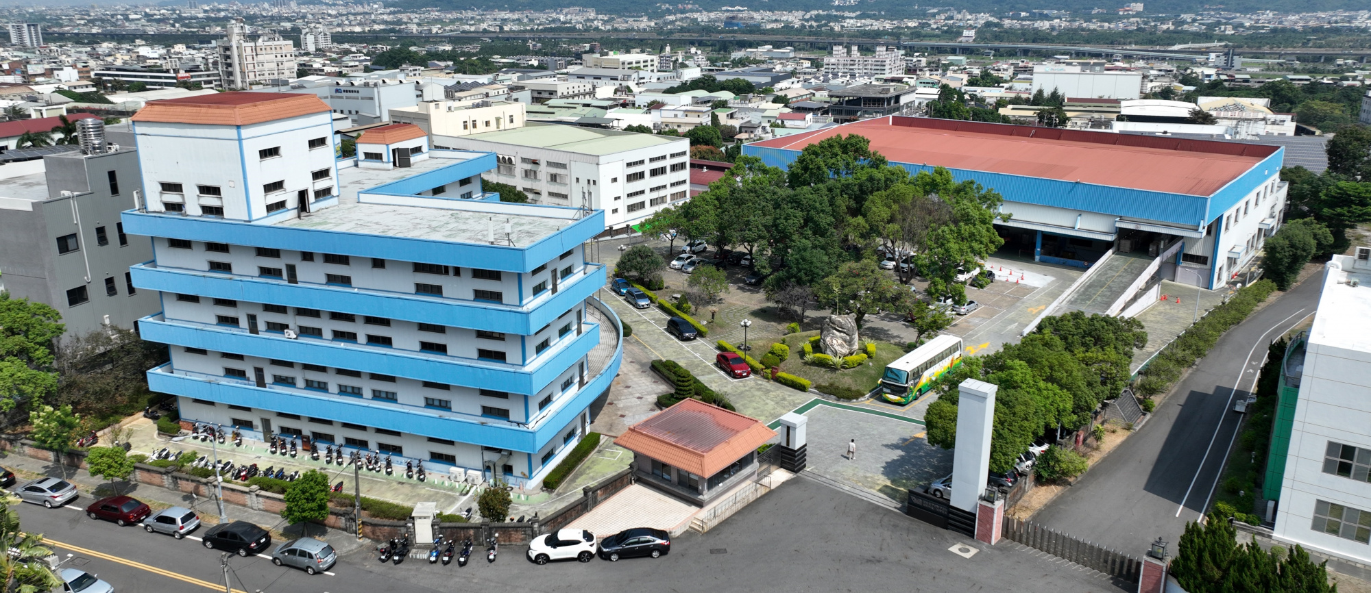
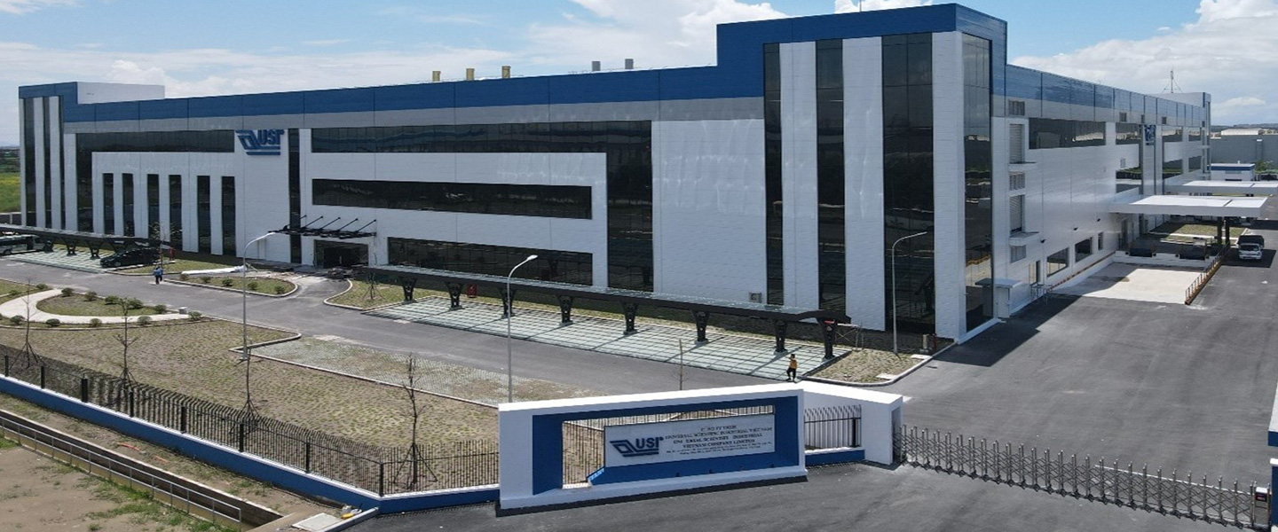
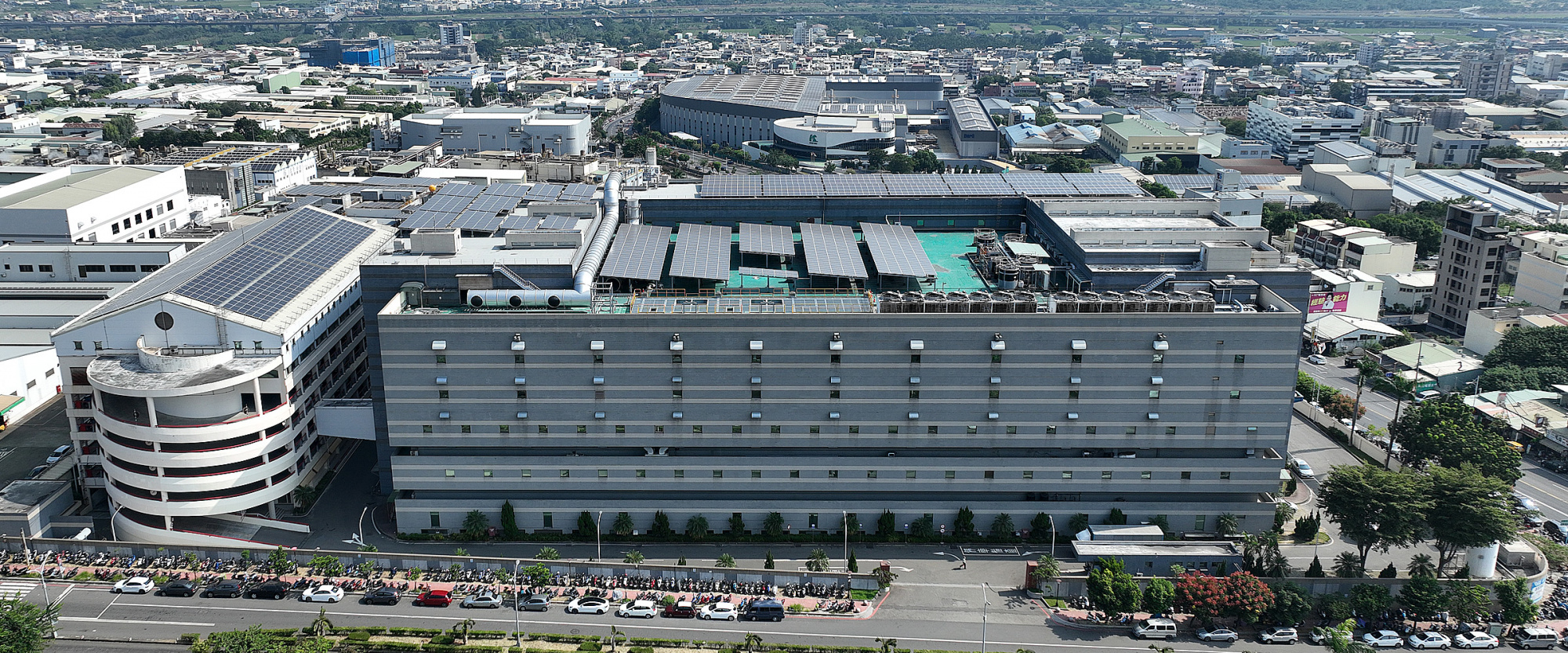
Taiwan-Nankang 1
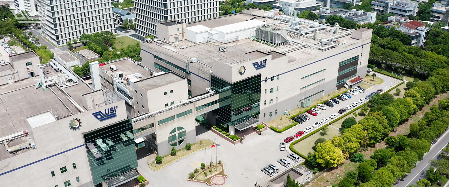
Universal Global Scientific Industrial Co., Ltd. (USI-Taiwan) is a subsidiary of Universal Scientific Industrial (Shanghai) Co., Ltd. USI-Taiwan is located in central Taiwan and has three facilities, the Tsaotuen site, the Nankang 1 site and the Nankang 2 site.
Nankang 1 site provides customers with electronic products and modules from concept development, design execution, software and hardware function verification, and product certification to manufacturing and other related services to assist customers in designing and manufacturing products with high reliability, high durability, and high quality and high performance.
The Nankang 1 site serves customers from the world's top brand companies with top-notch production equipment and a professional team, combined with excellent R&D, system integration and manufacturing capabilities. In recent years, it has also been vigorously promoting intelligent automation to optimize the existing manufacturing process through modularization and rapid switch of the production line to meet a small number of diverse needs. It dedicates to improving productivity, flexibility, efficiency, quality and cost-effectiveness, quickly responding to customer orders and markets, and meet customers' expectations of reducing manufacturing costs and perfect quality.
Nankang 1 site has sophisticated design and manufacturing experience in products/technology in the following fields. It can provide customers with high-value-added services and products with excellent response, efficiency and quality. In addition to providing customers with mass production of products, the Nankang site also has high flexibility in handling small and complex products.
- Wireless communication
- Computer and storage
- Consumer
- Industrial
- Automotive electronics